

=
Passive and active chips can be embedded in PCB using two basic processes: face-down and face-down. The two variants differ in the way components are connected to the outside world and use different materials and processes. Figure 1 outlines these two approaches.
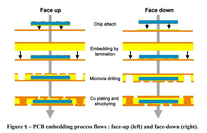
In the front process, the component is placed on the carrier material, and the contact pad of the component can be seen after assembly. This method provides some very good thermal performance and is very suitable for power module embedding. Processing constraints are encountered when trying to embed components with variable thickness. After embedding, the dielectric thickness between the component surface and the external copper surface remains unchanged, which poses a challenge to the subsequent micro-laser drilling and copper plating technology, especially in the case of via filling.
In the face-down process, the component and the component image are assembled together into the carrier material. Normally, screen-printed non-conductive adhesives are used as carriers for fixing components. This method has several advantages: good thickness control of dielectric materials between components and carriers, and good registration accuracy in assembly process. The reason for the improvement of alignment capability comes from the fact that the camera of the assembly machine can see the image of the component, so it can be aligned before the assembly is completed.
In frontal technology, the camera is aligned to the contour of the component.
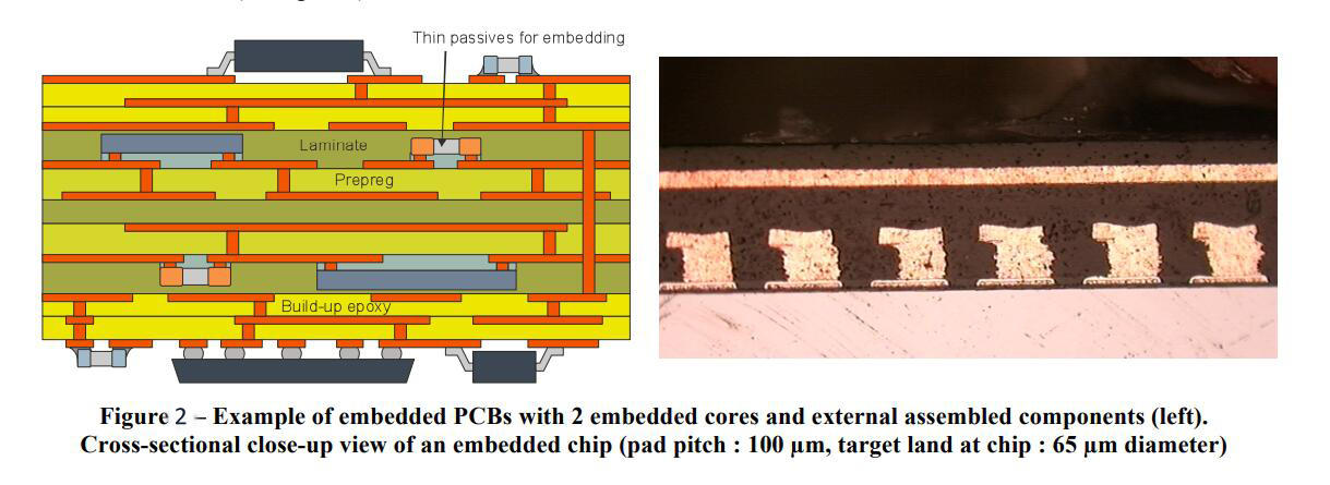
Using face-down technology, several components of different thickness can be embedded into the FR-4 core. The prepreg used for embedding is removed to form a cavity around the assembly. Prepregs with openings are stacked to the height of the assembly and are provided with non-openings at the top. By opening the dielectrics to various heights of the components, usually ranging from 100 to 350 um, it is easy to achieve different thickness embedding. Then, the embedded kernel can be used as the standard inner core and included in the PCB multi-layer structure. External SMD components can then be assembled on both sides of an embedded PCB to form very high-density modules/components (see Figure 2).
Embedded capacitors have many advantages, such as saving surface space, improving the product rate of device assembly, reducing power supply noise, reducing electromagnetic interference, simplifying circuit board design, and also raising higher challenges to equipment processing technology.
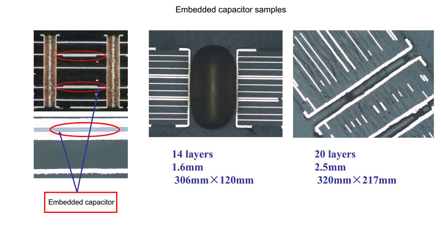
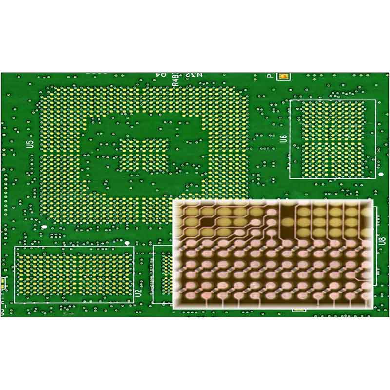
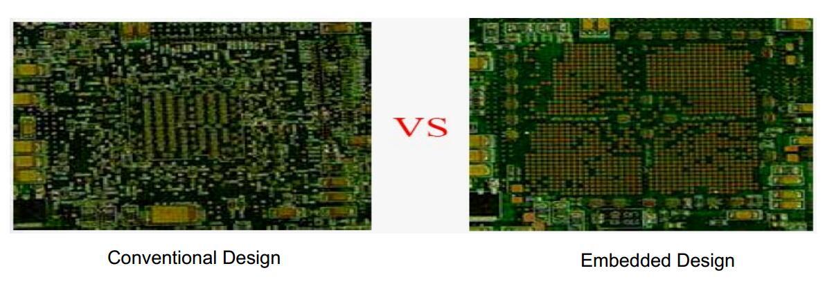
◪ Reduce surface mounting area by embedding chip components (resistors/capacitors)
◪ Improve electrical performance by shortening the wiring distance between surface-mounted ICS and embedded components
◪ Shorten the space between components and better heat resistance can be achieved by using a connection between the laser through holes and the copper-plated component terminals






Copyright © 2025 Rocket PCB Solution Ltd. | All Rights Reserved Sitemap Friendship link: CNC machining heat sink