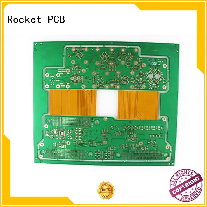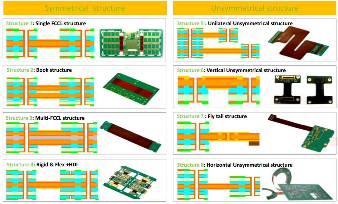


These PCBs
integrate flexible PCBs and rigid PCBs. Because the connection between
layers does not require connectors, they are ideal for digital devices
that are susceptible to noise. In addition, these PCBs can be designed
to create thinner devices with no-connector and three dimensions.
Rigid-flex
printed circuit boards can help you reduce space and ensure that your
products are able to withstand harsh conditions. Also, they are
cost-effective.
A rigid-flex format allows you to use fewer
interconnecting segments to take on more challenges. So the rigid-flex
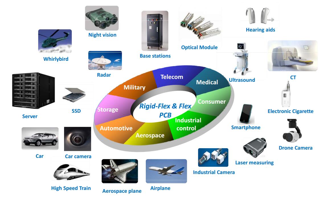
PCB is a very flexible solution to many design problems. They are
suitable for industries ranging from hearing aids to night vision
mirrors.


Rocket PCB is an innovative manufacturer focusing on electronic manufacturing. Rocket PCB is dedicated to spending 10 years of efforts advancing itself. We develop, produce and sell numerous successful high-quality products, including rigid, rigid-flex, HDI, any layer, Flex, large-size, embedded, RF, LED, backplane, metal substrate, ceramic substrate, IC structure, high-frequency, heavy copper. High quality and high reliability.

SPECIALIZED MANUFACTURING
Conductive materials and core-to-core bonding
Embedded components
RF connector attachment
Laser direct imaging (LDI)
Laser etching
Laser forming
Multi-level cavity construction
Plated cavities and edges
Composite/hybrid Structures
N+N dual press-fit
Dual-drill
Bonding on metal core
Bulid-up HDI
Long-short and staged gold finger
A wide range of professional manufacturing solutions, can be used for thermal energy (CTE) structural coefficients, thermal challenge design and application, extreme and unique HDI structures, and RF control
A wide range of professional manufacturing solutions, can be used for thermal energy (CTE) structural coefficients, thermal challenge design and application, extreme and unique HDI structures, and RF control
A wide range of professional manufacturing solutions, can be used for thermal energy (CTE) structural coefficients, thermal challenge design and application, extreme and unique HDI structures, and RF contro

CAPABILITIES
3mil line and space
4mil laser defined vias
6mil chip-on-board
6mil mechanically drilled vias
Conductive and non-conductive via fill
Dual backdrilling
Sequential lamination
Mixed dielectric
Heatsink Bonding
Heavy copper/thermal vias
Blind/buried vias
Stacked and staggerd microvias

Design Rules Check(DRC)
Electrical Testing
Automated Optical Inspection(AOI)
X-Ray
Plating thickness testing
Metalized vias inspection
Thermal shock testing
Surface peelability testing
Impedance control testing
100% visual inspection
Solderability testing
Ionic cleanliness testing
Metallographic microscopic analysis
High voltage testing
Insulating resistance testing

FEATURES
PTFE
High speed/low loss
High temperature
Low CTE
Lead-free, HASL, ENIG, EPENIG, Immersion Silver, Tin, Gold finger
Combination surface finished
Copper-filled microvias
| Design | Manufacturing | Quality Control |
|---|---|---|
| > High TG Rigid material, High reliability Flexible material | > Automatic Pasting Machine | > Check the quality of hole copper plating |
| > Using no‐flow PP and common flow PP | > High temperature lamination machine | > 100% AOI to inspect the desmear result of Micro Via |
| > Partial Coverlay, PTH can’t drill in the adhesive | > High speed drilling machine | > 4 wire low resistance test |
| > PI Conditioner production line | ||
| > Horizontal Desmear and Horizontal PTH | ||
| > Copper via filling plating line and Pulse plating line | ||
| > Vacuum resin filling machine |
Design
> High TG Rigid material, High reliability Flexible material
> Using no‐flow PP and common flow PP
> Dedicated design regulation of no‐flow PP filling copper
> Different squeezed‐out PP lengths use different manufacturing methods
> Partial Coverlay, Coverlay stretch into rigid part with 0.8‐2.0mm
Manufacturing
> Automatic Pasting Machine
> Plasma Machine
> High temperature lamination machine
> Different Rigid‐Flex structures use different buffering material
Quality Control
> Use micro section to check the blister and delamination after lamination
> Squeezed‐out PP of Rigid‐Flex interface less than 1.5mm
> Lead free reflow and thermal stress test, no delamination Plasma Machine
| Design | Manufacturing | Quality Control |
|---|---|---|
| > Different structures have different working panel sizes | > LDI exposure machine | > Check the registration coupon of layers after lamination |
| > Different lamination position methods | > Firstly make flex material pattern, after coverlay lamination to make rigid material pattern | > Check breakout of pad after drilling |
| > Regulation of copper designed in the spare of working panel | > ATP punch machine, INSPECTA target drill machine, divide the boards into different groups to manufacture | > Check soldermask on pad after soldermask process |
| > Registration coupon of layers | > BURKLE high temperature lamination machine | |
| > Soldermask Split exposure machine |

Copyright © 2019 Rocket PCB Solution Ltd. | All Rights Reserved Sitemap Friendship link: CNC machining heat sink